ASML High-NA EUV: When Chipmaking Feels Like Magic
Table of Contents
Some technologies eventually become so normal that we almost forget how absurd they really are.
SpaceX now sends a rocket into orbit roughly every two to two and a half days on average. Internet from space is no longer science fiction, but a product with an app, a router, and a monthly subscription. We carry supercomputers in our pockets, stream videos on trains, pay contactless, make calls over IP networks, and expect everything to simply work.
With many of these technologies, I can at least imagine what is happening at the core. I understand how routing works, why subsea cables are the real backbone of the internet, and how TCP, DNS, BGP, fiber optics, satellite links, and firewalls interact. Even with rockets and engines, enough videos, cutaway drawings, and physics let me build a mental picture. Not at an engineer’s level, but enough that it no longer feels completely mystical.
Modern chip manufacturing is different.
Of course, I roughly know that chips are made of silicon, that transistors are getting smaller, and that wafers are exposed, etched, and coated. But as soon as you really enter the scale of modern lithography, my understanding tips over. Then we are no longer talking about “small,” but about structures so far below my normal imagination that the whole thing starts to feel like magic again.
And then there is this machine from ASML: High-NA EUV. A system that costs more than 400 million dollars. Larger than a double-decker bus. So complex that it travels around the world in modules, is reassembled on site, and can only operate in the cleanest environments humans can build. A machine that hits tiny droplets of liquid tin tens of thousands of times per second with lasers, creates extreme ultraviolet light from them, and uses that light to print patterns on wafers that later become CPUs, GPUs, AI accelerators, and smartphone chips.
There is this thought: what you do not understand looks like magic. That is exactly how EUV lithography feels to me. But the fascinating part is this: once you start to understand it, it does not become less magical. It becomes even more absurd.
“When you do not understand a technology, it feels like magic.”
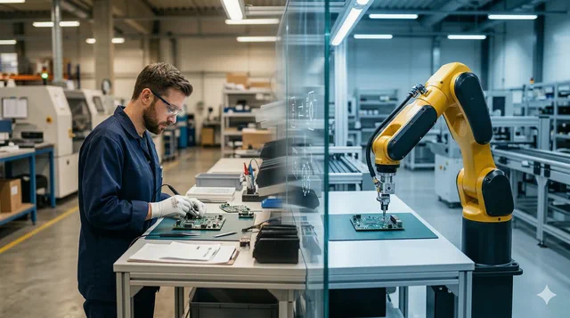
For me, this image captures why the machine grabs me so much: inside, it looks like an exposed piece of the future, while at the customer site it later stands more like a large white industrial box inside the fab.

A Few Numbers You Have To Read Twice
Before getting into the physics at all, it is worth looking briefly at the scale. Not because big numbers automatically mean good technology, but because otherwise this machine remains too abstract.
A High-NA EUV machine is not simply shipped. It is assembled at ASML, qualified, taken apart again, and transported to the customer in modules. Depending on how you count, behind it are around 800 to 5,000 suppliers. Large subsystems are built in several countries, come together in Veldhoven, and then travel onward to the fab: roughly 250 containers, 25 to 30 trucks, and seven Boeing 747s for a single machine.
On top of that, there are about 100,000 individual parts, around 40,000 screws, roughly 3,000 cables, and more than two kilometers of lines or hoses. Connecting it at the customer’s site requires more than 2,000 electrical connections. This is no longer “a device.” It is a small industrial ecosystem that happens to have one task: controlling light so precisely that modern chips can be made from it.
The manufacturing itself also does not sound like normal mechanical engineering. Around 2,000 people work in the EUV factory, and they do so 24/7. A High-NA machine takes roughly one and a half years until it is built, tested, and qualified. And even then it is not “finished” in the sense of a product you simply put on a pallet. It is dismantled again and only then travels to the fab.
Even the environment is extreme. ASML’s cleanroom is described as having a maximum of about 10 particles per cubic meter at 0.1 micrometers. In this comparison, a very clean operating room is at about 10,000 particles per cubic meter. And we are talking about particles much smaller than pollen or fine dust.
Inside, it gets even more absurd. The machine fires at tiny tin droplets about the size of a blood cell. For this, a CO2 laser is brought through several amplifiers to roughly 20,000 watts. These droplets are hit tens of thousands of times per second. In newer sources, there are three laser pulses per droplet: first shape it, then thin it out, then turn it completely into plasma. At 50,000 droplets per second, that mentally becomes 150,000 precise laser hits per second. And the whole idea is not to hit “most of the time.” The system has to place those hits reliably at industrial scale.
The movement inside the scanner is also absurd. The reticle, the mask with the chip pattern, is not gently moved around. Accelerations are above 20 g; for the EXE platform, ASML even names 32 g for the reticle stage. That is roughly equivalent to a race car accelerating from 0 to 100 km/h in 0.09 seconds. At the same time, the overlay of chip layers has to be right at the nanometer scale.
And then there is this image that I can hardly get out of my head: imagine a tiny laser sitting on the side of a mirror. The beam goes all the way to the Moon. There is a coin lying there. The mirror control is so fine that you can not only roughly “hit the coin,” but decide whether the beam lands on one side of the coin or the other. That is the scale of the angular control, in the picoradian range. Comparisons like that are simplified, of course. But they help you feel the precision. We are not talking about “very accurate” in the normal mechanical engineering sense. We are talking about an industrial system where a displacement of just a few atoms already matters.
What ASML Actually Builds
ASML does not build chips. That is important. ASML builds the machines that companies like TSMC, Samsung, Intel, SK hynix, Micron, and others use to place the finest patterns on silicon wafers.
TSMC stands for Taiwan Semiconductor Manufacturing Company. Many people know Apple, Nvidia, AMD, or Qualcomm as chip brands. TSMC is often the factory behind them: the contract manufacturer that turns those designs into real chips.
A modern chip is basically an artificial city of electrical switches: a nanoscale computing city with many layers and hundreds of kilometers of wiring. At the very bottom sit billions of transistors. Above them are layers of wires, insulators, contacts, and tiny structures that connect everything. Some chips have up to around 100 layers, and each one has to fit extremely precisely onto the previous one. If two layers are shifted even minimally against each other, the chip is not simply “a bit worse,” but potentially scrap.
The central technology for this is called photolithography. In very simplified form, one cycle works like this:
- Material is deposited on a silicon wafer.
- A light-sensitive coating, the photoresist, is applied on top.
- A lithography machine projects a pattern onto this coating.
- The exposed area changes its chemical properties.
- After that, the wafer is developed, etched, coated, or doped.
- The process repeats for the next layer.
That almost sounds banal: you take light, a mask, and a sensitive surface. In principle, it is photography. Only the photo at the end is not an image, but part of a processor. And the “pixels” sit at scales where dust, heat, vibration, air molecules, chemical side effects, and the tiniest optical errors become real opponents.
ASML’s machines are projection systems. Light carries the pattern of a mask, also called a reticle, through optics onto the wafer. The optics shrink and focus the pattern. Then the machine moves the wafer onward and exposes the next area.
So the real question is: how small can you print with light?
The Problem: At Some Point, Light Is Too Coarse
In lithography, there are two big levers: the wavelength of the light and the numerical aperture of the optics. A shorter wavelength helps print smaller structures. A larger numerical aperture means the optics can collect and focus light from a wider range of angles. That also improves resolution.
For a long time, the industry got very far with DUV lithography. DUV stands for Deep Ultraviolet. Argon fluoride light with a wavelength of 193 nanometers became especially important. For years, it was the workhorse technology for advanced chips. With tricks such as immersion lithography, better masks, computational lithography, and multi-patterning, the industry squeezed more out of this technology than seemed reasonable.
But at some point, light is simply too long-wavelength for what you want to print. When the structures approach the wavelength, the light diffracts, interference becomes brutally important, and the pattern on the mask is no longer what cleanly lands on the wafer.
You can compensate for that to some extent with software, mask corrections, and multiple exposures. That is exactly what the industry did for years. But multi-patterning is expensive, slow, and prone to errors. When one critical layer becomes two, three, or four exposure steps, process time, mask costs, and risk all rise. Every additional step is another opportunity to lose yield.
So the industry needed shorter light.
EUV, Extreme Ultraviolet, works at 13.5 nanometers. That is more than 14 times shorter than 193 nm DUV, roughly the width of five DNA strands next to each other. In theory, that makes it possible again to print much finer structures. In practice, it starts a long list of problems that sounds so absurd that you understand why many people considered EUV unrealistic for decades.
13.5 nm light is absorbed by almost everything. By air. By glass. By normal lenses. By normal mirrors. You cannot simply send it through a nice optical system. The entire system has to operate in vacuum, and instead of lenses you need extremely special mirrors.
In other words: to build smaller chips, the industry had to invent a light source that practically does not exist on Earth, build optics smoother than anything normal humans ever touch, and then make the whole thing stable enough to earn money in a factory 24/7.
That was the bet.
The Long Bet On EUV
The story does not begin with High-NA, but with the question of whether lithography with such short-wavelength radiation is even possible.
In the 1980s, Japanese researcher Hiroo Kinoshita worked on the idea of using very short-wavelength radiation to print structures. The problem was immediately clear: this kind of light cannot be guided with classical lenses. It gets swallowed. The solution could only work through mirrors, but not normal mirrors. It needed multilayer mirrors, where many extremely thin layers are arranged so that the reflected waves add constructively.
Kinoshita produced early images, but at first he was not taken seriously. The skepticism was not simply ignorance. It was technically understandable. The light source was too weak. The mirrors were too difficult. The machines would have been too slow. And each one of those points would have been enough to kill a product.
At the same time, American national labs, including Lawrence Livermore, were working on X-ray and EUV-adjacent technologies, originally for entirely different reasons. Research from the environment of fusion and weapons physics delivered knowledge about multilayer mirrors and short-wavelength radiation. Then came the question of whether something useful could be built with that knowledge. That is exactly where one of the early paths toward EUV lithography came from.
In the 1990s, EUV became a real industry project. US labs, Bell Labs, Intel, Motorola, AMD, and others were involved. After government funding disappeared, chip companies continued investing themselves, because everyone could see that if 193 nm lithography eventually was no longer enough, a new answer would be needed.
Around the year 2000, there was an important prototype, the Engineering Test Stand. It showed that EUV could print patterns in principle. This test stand generated 9.8 watts of EUV light and could print 70 nanometer structures. But it was nowhere near fast enough. About ten wafers per hour is a lab success. A real fab needs hundreds of wafers per hour, day and night, with high availability, usable yield, and controllable costs.
This is exactly where science separates from industrialization.
A laboratory proof is one thing. A machine that a chip manufacturer includes in a multi-billion-dollar roadmap is something completely different.
One especially brutal bottleneck was the light budget. EUV mirrors do not reflect everything. When light passes through several mirrors and the reticle, less remains after every contact. At around 70 percent reflectivity per mirror, only a few percent of the photons remain after many reflections. That is why the light source was not just a component. It was the difference between “interesting experiment” and “industrially usable machine.”
Many companies dropped out or lost faith. In the end, ASML was the one that mostly remained.
That is remarkable because ASML itself once started small: a Philips spin-off in the Netherlands, at the beginning more of a shaky bet than a global monopolist. But ASML had two things: extreme focus on lithography and the willingness to share the risk with partners. ZEISS took on the optics. ASML integrated the system. Later, key technologies around the light source were also pulled ever more tightly into ASML’s world.
EUV was not a single invention. EUV was a chain of thousands of “almost impossible, but maybe still possible” problems.
As a supplement to this development story, this deeper introduction fits best here:
The Technical Impossibilities
Problem 1: How Do You Build A Sun Into A Machine?
You do not generate EUV light at 13.5 nanometers with a normal lamp.
ASML uses a laser-produced plasma source. In the basic principle, tiny droplets of liquid tin are generated. ASML publicly describes tin droplets about 25 micrometers in size, coming out of a generator at around 70 meters per second. That is roughly 250 km/h. These droplets are hit by laser pulses tens of thousands of times per second.
The first pulse flattens the droplet, almost like a tiny pancake. Then a much stronger pulse hits the tin and turns it into hot plasma. In newer explanations of current machines, the pulse sequence is described even more finely: pre-pulse, another pre-pulse to thin out the tin cloud, then the main pulse. Three hits happen in roughly 20 microseconds. The purpose remains the same: extracting as much usable EUV light as possible from as much tin as possible.
The plasma is unimaginably hot: around 220,000 degrees Celsius or Kelvin, roughly 40 times hotter than the surface of the Sun. From this plasma come photons with the desired EUV wavelength.
That alone is absurd. But it is not enough to hit one droplet once. The machine has to do it constantly. 50,000 times per second. If three pulses are needed per droplet, you end up with 150,000 laser pulses per second that have to fit in time and space. In newer roadmaps and statements, the direction even goes toward 60,000 and later 100,000 droplets per second.
And those droplets cannot be just anywhere. They have to be the same size, the same speed, and at the right place at the right time. The machine observes them, calculates their flight, and fires the laser so that the pulse lands exactly. The image for that: a golf ball in a storm has to fall into a distant hole, every time, without misses.
This is one of the points where my brain briefly checks out. Not because the principle is impossible to understand, but because the industrial repeatability is so unbelievable. An experiment is allowed to be spectacular. A fab machine has to become boringly reliable.
Problem 2: Tin Is The Solution And The Enemy At The Same Time
Why tin at all?
Early EUV sources used xenon, among other things. That worked, but the efficiency was poor. A large part of the energy did not end up in the desired 13.5 nm radiation. Tin is a better fit because it can generate EUV light much more efficiently in this range.
But tin creates a new problem: where does the material go?
That sounds banal, but it is an existential problem for the machine. Just one nanometer of tin on the collector mirror could be enough to take that mirror out of operation. At the same time, the source does not move symbolic amounts of tin through the system over its lifetime, but a lot of real tin. So the mirror has to stay almost perfectly clean while tiny tin-plasma explosions happen right next to it 50,000 times per second.
The machine is not symbolically shooting at these droplets. It vaporizes and tears them apart. But right nearby sits the collector mirror, an extremely expensive and extremely sensitive mirror that has to collect the EUV light. If tin builds up there, the source loses efficiency. If the mirror gets too dirty, the machine stops.
So ASML had to not only generate light, but also prevent its own light source from destroying itself.
Part of the solution is hydrogen. There is low-pressure hydrogen in the source chamber. It slows and cools tin residue and helps convert tin chemically into gaseous compounds that can be removed. But that is not a simple filter trick either. The tiny plasma explosions heat the hydrogen and create shock waves. You can imagine them as mini-supernovae forming inside the vessel 50,000 times per second. The engineers had to understand how much energy ends up in the gas, how fast it has to flow, and how to get enough protection without absorbing too much EUV light again.
This part shows exactly how unromantic magic is in practice. There is no wizard sitting at the lever. There are engineers looking at measurement data, seeing shock waves in the gas, comparing them with formulas from explosion physics, and realizing: we need to flush hydrogen through this system at absurd speeds. The order of magnitude is around 360 km/h of gas flow, more than a Category 5 hurricane, even though the density inside the system is of course much lower.
And even that did not solve everything. Another stumbling block was that the collector still degraded too quickly despite hydrogen. The breakthrough came from an observation: when the machine was opened, the mirror apparently became cleaner. The reason was oxygen. So the team experimented with tiny amounts of oxygen in the system, enough to improve the cleaning process, but not so much that the vacuum system and EUV transmission suffered.
That is the kind of engineering I love: the big idea is important, but in the end, the person who takes a strange detail seriously often wins.
Problem 3: Mirrors That Should Not Really Exist
EUV does not pass through glass lenses. So EUV lithography works with mirrors.
But mirrors do not reflect EUV the way a bathroom mirror reflects visible light. EUV mirrors consist of extremely precise layer systems, typically molybdenum and silicon. Many wafer-thin layers are tuned so that they reflect as much light as possible exactly at 13.5 nanometers.
Even then, a single mirror reflects only part of the light. When the light is reflected several times, the remaining power shrinks quickly. That is why the light source remained the bottleneck for so long. More light at the beginning means more usable light at the wafer.
At the same time, the surfaces of these mirrors have to be brutally smooth. For modern EUV mirrors, ASML talks about smoothness in the range of dozens of picometers. A normal household mirror is brutally rough by comparison: figuratively speaking, surface irregularities in the order of thousands of silicon atoms, while early EUV mirrors had to be atomically smooth.
The scale comparisons stay with you: if a Low-NA EUV mirror were scaled to the size of Germany, the highest irregularity would be roughly one millimeter. With High-NA, the image gets even more extreme: if the mirror were as large as Earth, the highest irregularity would be about as thick as a playing card.
That sounds like marketing, but behind it is hard physics. At a wavelength of 13.5 nm, a small irregularity is not “a scratch.” It scatters light, eats contrast, and degrades the image. The mirrors not only have to be smooth, they also have to be controlled in position, shape, and temperature.
ZEISS plays a central role here. For High-NA EUV, the optics became even larger and heavier. ZEISS describes the projection optics for High-NA as having more than 40,000 parts and weighing around twelve tons. That is seven times the volume and weight of the established EUV projection optics. At the same time, individual optical elements have to be aligned and controlled with nanometer precision.
That is the next mind-bender: you build something gigantic so you can print something tiny.
How The Machine Works
For the technical process itself, the official ASML video fits exactly here. It shows the High-NA platform, the anamorphic optics, the faster stages, and why the TWINSCAN EXE was built for future chip generations.
What High-NA Changes Compared With Normal EUV
ASML’s first commercial EUV machines, the NXE systems, work with a numerical aperture of 0.33. High-NA, meaning the EXE platform, raises this NA to 0.55.
Optically speaking, the idea behind this is simple: a larger NA captures light from a wider range of angles. That allows the system to image finer details. ASML gives a resolution of 8 nm for the TWINSCAN EXE:5000. Compared with NXE systems, it is supposed to enable single-exposure structures that are 1.7 times smaller, and therefore much higher transistor densities.
But here too, the catch arrives immediately.
When light hits the reticle at larger angles, new problems appear. The reticle reflects worse at these angles, and a simple “let’s make everything bigger” would break the entire mask infrastructure of the industry. The solution is called anamorphic optics.
Instead of shrinking the pattern equally in both directions, High-NA shrinks it differently: 4x in one direction and 8x in the other. That allows the industry to keep working with traditional reticle sizes while still getting the benefits of the higher NA.
The price: the exposure field is smaller. Each wafer needs more exposures. To keep that economical, wafer and reticle stages had to become much faster. ASML names more than 185 wafers per hour for the EXE:5000 and a roadmap toward 220 wafers per hour. Accelerations are above 20 g; for the EXE platform, ASML specifically names 8 g for the wafer stage and 32 g for the reticle stage.
You have to imagine this for a moment: inside this machine, a pattern is transferred with nanometer precision while parts are moving with accelerations that sound more like motorsport or aviation. And still, the overlay of the layers is only allowed to be off by a few atoms. For this overlay precision, about one nanometer is cited, roughly five silicon atoms.
The Moon-and-coin image fits here once again: if the mirror control is fine enough that an imagined laser beam over Moon distance can distinguish between two sides of a coin, then you begin to understand what picoradian accuracy means. The machine does not only have to print small. It has to place layers over and over again so precisely that an error in the range of individual atomic layers becomes relevant.
That is the real High-NA point: not just printing smaller, but printing smaller without destroying the production economics.
How One Exposure Step Really Fits Together
If you look at the machine as a process, it becomes a little more graspable.
First comes the wafer. It was prepared beforehand in other tools: cleaned, coated, possibly given thin material layers, and covered with photoresist. These pre- and post-processes are just as much part of chip manufacturing as lithography itself. ASML’s machine is not the entire fab, but one of the most critical tools in it.
Then comes the mask. It carries the pattern that should later appear on the wafer. But this pattern is not simply a naive drawing of the target image. Because of diffraction, chemistry, resist behavior, and process distortions, such a direct pattern would land incorrectly. That is why the industry uses computational lithography and Optical Proximity Correction. Put simply: the mask is intentionally drawn “wrong” so the physical process prints the right result in the end.
Then the light source generates EUV photons from the tin plasma. A collector mirror gathers as much of that light as possible and sends it onward into the scanner.
In the illuminator, the light is shaped. Then it hits the reticle. Because EUV does not pass through a mask the way visible light passes through a slide projection, the reticle is reflective too. The light picks up the pattern and continues into the projection optics.
That is where the actual imaging onto the wafer happens. Mirrors shrink and correct the image. With High-NA, this happens anamorphically, meaning differently in two directions. At the same time, the stage moves the wafer so that one field after another is exposed.
After exposure, the photoresist is developed. Depending on the resist type, exposed or unexposed areas remain. Then follow etching, deposition, doping, cleaning, and further steps. For the next layer, the cycle starts again.
The difficulty is not in one single step, but in the sum:
- The EUV light has to be strong enough.
- The mirrors must not get dirty.
- The optics have to remain stable.
- Wafer and reticle have to move extremely fast and extremely precisely.
- The layers have to fit on top of each other with nanometer overlay.
- The whole thing has to run in a real production environment.
Each point alone would be a world-class engineering problem. ASML has to solve all of them at the same time.
Why The Story Is So Fascinating
What fascinates me about ASML is not only the machine itself, but also the tension in its development.
For decades, EUV was not a sure thing. There were prototypes, but not enough light. There were better light sources, but tin destroyed the mirrors. There were mirrors, but not enough throughput. There were breakthroughs, but the market kept moving the finish line because DUV with multi-patterning held on longer than expected.
That is an important point: ASML was not working in a calm laboratory on a clear future. The company had to build a technology while customers doubted, wafer-per-hour targets rose, costs exploded, and alternatives were pushed further and further.
One moment especially stays with me: in the early 2010s, ASML had not yet reached the goal with current EUV, but was already working on the next generation, High-NA. That is actually absurd. You do not yet have current EUV cleanly in production, but you already start the next, even more difficult platform.
From a normal project management perspective, that sounds unreasonable. From a technology perspective, it was probably necessary. If you only start High-NA once Low-NA runs perfectly, you arrive ten years too late.
This kind of bet always looks logical in hindsight. In real time, it looks more like madness with a budget.
Intel, Samsung, and TSMC invested directly in ASML to help carry this development. The scale: around 4.1 billion dollars from Intel and another combined 1.3 billion dollars from Samsung and TSMC. That alone shows how central the machine was for the future of the industry. Without EUV, Moore’s Law would not simply have died, but the cost and complexity of further scaling would have become much harsher.
One especially strong moment came in 2015: ASML finally had to show customers in Korea 200 watts of EUV source power. Patience was thin. When the ASML people boarded the plane, the experiment was still running. When they got off, the first results were there: 200 watts. That is how close this technology was at decisive points.
And now, in 2026, High-NA is no longer just a lab dream. ASML has shipped the first systems, Intel has installed the first commercial High-NA system in Oregon, imec and ASML operate a joint High-NA lab in Veldhoven, and ASML had already recognized revenue for two High-NA systems by the end of 2025.
Still, the sober part matters: a 400-million-dollar machine does not win because it is impressive. It only wins if it improves the equation in a fab: fewer masks, fewer process steps, better yield, shorter cycle time, or new structures that otherwise would not be economically viable.
Even magic has to survive Excel in the semiconductor industry.
The Infrastructure View
As a network and security person, I automatically look at dependencies. And with ASML, the dependency is almost unsettling.
ASML is currently the only supplier of EUV lithography systems. DUV has competition, EUV practically does not. At the same time, the most advanced chips depend on exactly this technology. That affects smartphones, AI accelerators, server CPUs, GPUs, high-bandwidth memory, networking technology, automotive, research, and military applications.
That makes ASML an infrastructure company, even though the company does not operate internet lines and does not own data centers. It sits deeper in the stack. Below cloud. Below AI. Below smartphone. Below network hardware. Below almost everything that scales digitally today.
The machine itself is also infrastructure in the extreme. A High-NA system consists of around 100,000 parts, about 3,000 cables, roughly 40,000 screws, and around two kilometers of hoses or lines. Depending on how you count, people speak of 800 global suppliers up to 5,000 supplier companies. The High-NA machine consists of four large subsystems that are built, among other places, in Connecticut, Germany, the Netherlands, and California. These parts first go to Veldhoven, are assembled and tested there, then taken apart again, and only then shipped to the customer.
The transport alone is almost its own logistics story: around seven Boeing 747s, 25 to 30 trucks, and depending on the count, about 250 containers. Those are the transport figures for a single machine.
This is not a single machine in the classic sense. It is a global ecosystem compressed into a machine.
And that is exactly why export controls, geopolitical tensions, and supply chains are not side issues here. Anyone who does not get EUV has to try to keep up with older techniques, more multi-patterning, more effort, and worse economics. That can work for individual nodes, but it changes the rules of the game.
What I Take From It
I wanted to write this article because I wanted to understand this machine. Not completely; that would be arrogant. But enough so that “this is magic” turns into a usable internal model.
My model now looks like this:
ASML High-NA EUV is not a magic machine. It is an extremely consistent answer to a physical limit.
People wanted smaller structures. So they needed shorter light. This light is absorbed by almost everything. So they built a vacuum system with mirror optics. The mirrors reflect only part of the light. So they needed a stronger source. The source creates light by turning tin into plasma. The tin dirties the mirrors. So you need hydrogen, oxygen, gas flow, sensors, and cleaning. The optics get larger. So you need High-NA, anamorphic imaging, faster stages, and even better correction models. And because every layer has to fit perfectly onto the previous one, everything has to be controlled in the nanometer range.
This is not one single brilliant idea. It is a tower of solved impossibilities.
Maybe that is exactly why this machine grabs me so much. It shows how far people can go when a goal is important enough and the economics eventually become large enough to finance what is actually unreasonable.
It reminds me a little of food. When you start thinking about where the food on your plate comes from, something ordinary suddenly becomes wild again. Especially here in Dubai, where practically everything is imported from all over the world. A strawberry or tomato looks simple until you think about seeds, water, fertilizer, climate, harvest, cold chain, quality control, transport, storage, and the supermarket. In the end, something lies on the plate that only feels obvious because thousands of steps worked beforehand.
With chips it is similar, only even more extreme. I am writing this article on a device whose processors were made possible by manufacturing chains like this. The AI that helps in the data center with correcting, structuring, or translating runs on chips that in turn are possible in this form only because of machines like this. It is a technical supply chain that lies so deep beneath our everyday life that we almost never see it.
Rockets look more spectacular. Subsea cables are more tangible. Networks are more familiar to me. But this machine hits something else: it feels like the point where physics, materials science, optics, mechatronics, software, chemistry, supply chain, and sheer stubbornness come together.
And yes, it still feels like magic.
But now a little less like unexplained magic and more like the kind of magic that happens when thousands of very good engineers refuse for decades to accept that something is supposed to be impossible.
Until next time,
Joe