As China Catches Up: Shenzhen, Huawei, and the Next Chip Era
Ai Security PersonalTable of Contents
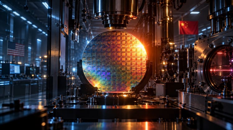
Somewhere inside a tightly secured laboratory in Shenzhen stands a machine that nearly fills an entire factory floor. It is designed to produce extreme ultraviolet light, the 13.5 nm radiation that only ASML has so far mastered in production-ready lithography systems. According to a Reuters investigation, the Chinese prototype has been operating since early 2025. It produces EUV light, but it has not yet exposed a functioning chip.
That distinction determines whether this is a historic breakthrough or merely a very large laboratory setup. A light source is not yet a scanner. A scanner is not yet economical mass production. Yet the machine apparently exists, and Huawei is said to coordinate the nationwide network of companies and research institutes that made it possible.
To understand why a telecommunications group from Shenzhen is suddenly involved in one of the most complex machines ever built, we have to return to the night of May 17, 2019. That was when He Tingbo sent a letter nobody at Huawei had wanted to receive.
The United States had placed Huawei on the Entity List. American companies could supply many products and technologies only with a license. For a company whose phones, networks, and servers depended on a global web of chips, software, manufacturing equipment, and patents, this was not a routine trade disruption. It was the emergency for which Huawei had prepared for years.
He Tingbo led HiSilicon, Huawei’s chip-design operation. Her internal letter described technologies that had been developed as reserves and stored in a metaphorical vault. Those “spare tires” now had to become the normal program overnight.
Seven years later, the same woman appeared at the IEEE International Symposium on Circuits and Systems in Shanghai. This time she was not merely explaining survival after sanctions. With Tau Scaling and LogicFolding, she presented a way for Huawei to compensate for part of its manufacturing disadvantage elsewhere in the system.
The technically interesting idea is simple: if China cannot manufacture the smallest transistors with the same machines as TSMC, Samsung, or Intel, it has to move data faster by other means, from the transistor all the way to the data center.
“Excluding China from key technologies buys time. It also gives China the strongest possible reason to eliminate that dependency for good.”
He Tingbo and the Moment the Reserve Was Needed
He Tingbo is not a manager who suddenly appeared with a marketing concept. Born in 1969, she studied semiconductor physics and communications engineering and earned a master’s degree from Beijing University of Posts and Telecommunications. She joined Huawei in 1996 and advanced from ASIC development through research, architecture, and supply-chain responsibility to the top of its semiconductor business.
That background matters. An ASIC is a chip designed for a specific application. Someone who started there in the 1990s and later ran HiSilicon knows the layers behind a finished processor: logic design, architecture, manufacturing partners, and a reliable supply chain.
HiSilicon was formed in 2004. It designs Kirin smartphone processors and Ascend AI accelerators, among other products, but historically did not own a complete manufacturing chain like Intel. A design becomes real only when EDA software, IP blocks, masks, foundries, lithography, deposition and etching tools, materials, memory, and packaging all fit together. After 2019, those dependencies became successive targets of US export rules.
What the Reserve Really Was
The spare-tire strategy is often attributed to He Tingbo alone. It makes for a neat story, but it is too simple.
Huawei founder Ren Zhengfei said in 2019 that he had spoken publicly about a “Plan B” for roughly a decade. He Tingbo’s letter made the reserve visible because it appeared on the night when an abstract risk became real. Her teams had developed many alternatives, while the doctrine itself came from Huawei’s wider leadership.
The idea was not autarky at any price. Huawei continued buying from partners such as Qualcomm wherever it could. The aim was redundancy: design critical chips internally, prepare alternative operating systems and software, qualify multiple suppliers, and preserve technical paths that could be more expensive or less elegant in normal times. A reserve that is never tested is only a slide deck. After 2019, Huawei had to fit its spare tires under load.
When an Emergency Program Became a Production Strategy
The Entity List was only the beginning. In May 2020, the US Department of Commerce expanded the Foreign-Produced Direct Product Rule. Certain chips manufactured outside the United States to Huawei or HiSilicon designs also required a license when specified American software or manufacturing technology was involved.
That struck the business model at its weakest point. HiSilicon could design excellent chips but relied on foundries such as TSMC to manufacture them. Modern foundries almost inevitably use American technology somewhere in design or production. A Chinese design therefore did not automatically become a freely available Chinese product.
Huawei lost smartphone market share and had to reorganize product lines. Years of preparation were not a magic shield. The controls inflicted real economic and technical damage and widened the gap to leading-edge manufacturing.
The Kirin 9000S in the Mate 60 Pro nevertheless showed in 2023 that slowed did not mean stopped. TechInsights identified a 7 nm-class chip made by SMIC on its N+2 process. It did not equal the leading 3 nm processes of the time, but it proved that Huawei and SMIC had pushed DUV lithography, complex multi-patterning, and domestic process development further than many observers expected.
Readers of our article on ASML’s High-NA EUV machine know the other side of this story. ASML uses 13.5 nm light, controls tin plasma and atomically smooth mirrors, and prints ever finer structures. Huawei cannot buy these machines, so it is trying to reduce its dependence on ever smaller features.
Tau Scaling: When Time Matters More Than Size
Moore’s law is often reduced to transistor counts doubling roughly every two years. Its historic benefit was broader: smaller transistors switched faster, consumed less energy, packed closer together, and enabled shorter connections. Performance became cheaper at the same time.
That relationship has weakened. Voltages no longer fall at the old pace, leakage and heat limit clock speeds, interconnects account for more delay, and leading-node development is extraordinarily expensive. Huawei also lacks normal access to the latest manufacturing.
He Tingbo’s answer is Tau Scaling. The Greek letter τ commonly represents a time constant. Instead of asking only how small a transistor is, Huawei asks how long information takes to reach the place where it is needed.
At transistor and local-interconnect level, parasitic resistance and capacitance matter. In a rough approximation, delay behaves like τ ≈ R × C. Long, thin wires have more resistance. Adjacent conductors form capacitances that must be charged and discharged. The larger the product, the later a signal arrives reliably.
At chip level, critical logic paths, cache hierarchies, memory access, and the network-on-chip join the problem. In servers, links between accelerators, memory, and CPUs matter. In a data center, protocol transitions, switches, optical links, and the time thousands of chips spend waiting become part of the same optimization target.
Tau Scaling does not abolish geometric scaling. It turns it into one method among several for saving time. The industry already co-optimizes chips, packaging, memory, software, and systems. What is strategically new is how explicitly Huawei directs that approach at a manufacturing disadvantage.
LogicFolding: The Chip Leaves the Plane
The most tangible part of Tau Scaling is LogicFolding. Imagine a dense city. Instead of extending roads ever farther, it places another active district directly above the first and connects them with many short vertical routes.
On a chip, the buildings are standard cells made of transistors. Many cells form combinational logic between registers, and the slowest relevant route limits the safe clock frequency. In a conventional design, active transistors occupy one plane with metal layers above them. LogicFolding distributes cells from one logical block across two active planes joined by very fine hybrid-bonding connections. To the design tools, they should behave as one three-dimensional circuit.
How the Shorter Signal Path Is Built
The process begins in chip design:
- EDA software analyzes millions of cells for critical paths, long wires, timing problems, and hot spots.
- Related standard cells may be placed on different active layers.
- Frequently communicating cells are positioned close together in three dimensions, shortening routes that would require detours in 2D.
- Hybrid bonding joins facing metal contacts and insulating surfaces at very fine pitch.
- Through-connections, power delivery, clock distribution, and redundancy connect the stack and compensate for isolated defects.
Huawei’s paper describes a 1.5 micrometer hybrid-bond pitch and alignment accuracy below 0.5 micrometers for the first Kirin implementation. LogicFolding is initially applied to selected critical paths rather than the entire design.
According to Huawei’s measurements, transistor density at the same manufacturing node rose from 155 to 238 million transistors per square millimeter, about 55 percent. The performance core’s energy efficiency reportedly improved by 41 percent and maximum clock frequency by almost 13 percent. In a representative core, total wire length fell by roughly 30 percent and the number of clock buffers by more than half.
Those are impressive figures, but they remain vendor claims until an independent laboratory measures a commercial LogicFolding chip. A Kirin scheduled for autumn 2026 is meant to provide the first production implementation.
Why This Is More Than Ordinary Chiplet Stacking
Multiple chips in one package are not new. AMD, Apple, TSMC, and others use sophisticated 2.5D and 3D packaging, usually connecting previously designed functional blocks or complete dies.
LogicFolding works at a finer level. Standard cells inside the same module may move across active layers, so placement and routing must be optimized in three dimensions from the beginning. Peking University is developing such a “True 3D” EDA approach. Its prototype treats multiple dies as one design space and jointly optimizes cell placement, vertical links, wire length, and thermal paths. Tests on open industrial designs reported about 30 percent less wire length than a coarser module-based 3D method.
Why LogicFolding Does Not Replace ASML
The tempting headline is that Huawei can now make 1.4 nm chips without EUV. That is not supported by the evidence.
Huawei says its high-end designs should reach transistor density comparable to a 1.4 nm process by 2031. That is a target for density and system performance, not proof of a 1.4 nm manufacturing process or physical features measuring 1.4 nanometers.
The often quoted number of 381 chips also needs context. He Tingbo writes that her team brought 381 chips for mobile devices, AI, vehicles, industry, and infrastructure into mass production between May 2020 and May 2026. They supplied experience for the broader Tau approach. The paper does not say all 381 used LogicFolding. It identifies the 2026 Kirin as the first production proof of that architecture.
LogicFolding can place more logic on the same footprint and shorten signal paths, but it does not make the underlying transistors finer. Each layer still requires lithography, deposition, etching, implantation, and many other steps. Older nodes generally need more area and energy for the same logic. Extra layers shift part of the problem into packaging and integration.
ASML therefore remains essential. Huawei is buying time while China simultaneously works on better DUV systems, domestic EUV components, and an end-to-end manufacturing chain.
Shenzhen’s Secret EUV Project
Reuters reported in late 2025 that a working EUV prototype in Shenzhen had been completed in early 2025. Former ASML engineers reportedly helped with reverse engineering, while components from older equipment and the secondhand market were studied, dismantled, and integrated into a new system.
Neither Huawei nor Chinese authorities confirmed the details. The investigation relies substantially on anonymous sources because the project is said to be classified. It should therefore be read as credible and detailed reporting, not as a publicly demonstrated and independently measured machine.
What the Prototype Must Achieve
An EUV machine is not simply a laser with a short wavelength. It is a chain in which every stage must pass enough light, precision, and stability to the next.
Tiny droplets of molten tin are struck by powerful laser pulses to form plasma. A small share of the resulting radiation is EUV light at 13.5 nm. A collector mirror must capture as many photons as possible without being quickly ruined by tin contamination.
EUV is absorbed by air and ordinary glass, so the optical path operates in vacuum and uses multilayer reflective mirrors instead of lenses. Light then hits a reflective mask. More mirrors reduce and project the pattern onto a photoresist-coated wafer while mask and wafer stages move quickly with nanometer precision. Measurement systems continuously correct position, focus, vibration, and thermal drift.
China must industrialize at least this chain:
- a powerful and stable tin-plasma light source,
- a collector that efficiently gathers light and survives contamination,
- extremely precise illumination and projection optics,
- masks, pellicles, photoresists, and metrology for 13.5 nm,
- high-dynamic wafer and mask stages with their control systems,
- software, process recipes, and service that repeatedly produce good wafers.
Reuters says the Shenzhen setup generates EUV light, but its optics remain substantially inferior to ASML and ZEISS systems and it has not produced a working chip. A laboratory source may emit photons yet remain too weak, unstable, or dirty for economical exposure. A complete optical path may form an image without reaching a fab’s required resolution, overlay, and throughput.
Why the Chinese Machine Became So Large
ASML optimized its systems for power, throughput, maintenance, and footprint over decades. The Chinese team reportedly tried to match similar dimensions, then built a much larger prototype when that failed.
For research, that is a sensible trade. Occupying a factory floor is cheaper than losing more years if the first goal is merely to make the physical chain work. For mass production, size is not arbitrary. Long optical paths are more sensitive to vibration, temperature, and alignment error, while more components create more failure points. The oversized setup shows that China may have made a difficult subsystem work, not that it already has a competitive ASML product.
Reverse Engineering, People, and the Limits of the Evidence
Reuters reported that recently retired, China-born former ASML engineers worked under aliases in the secured laboratory, that current ASML employees had been approached by Huawei recruiters, and that around 100 young graduates dismantled, documented, and rebuilt components.
That sounds like a spy thriller, but the language matters. Former employees may generally change jobs, and reverse engineering is not automatically theft. Confidential documents and trade secrets remain protected. Reuters found no evidence of legal action against people involved in the Shenzhen project. ASML said former staff remain bound by confidentiality obligations and that it acts against trade-secret theft.
Experienced engineers are valuable even without a secret drawing. They know dead ends, contamination patterns, control problems, and useful measurements. Reverse engineering does not remove the physics, but it can remove failed experiments.
One key figure is Lin Nan, a former ASML light-source manager. His team at the Shanghai Institute of Optics and Fine Mechanics reportedly filed eight EUV light-source patents in 18 months. The Changchun Institute of Optics, Fine Mechanics and Physics is said to have integrated the radiation into the optical system.
China’s organizational method is visible here: bring experience home, understand imported or used equipment down to component level, divide tasks among specialized institutes, and use Huawei as an integrator. This is less a copy of one finished machine than an attempt to reconstruct ASML’s international supplier network inside China.
2028, 2030, or Much Later
Reuters says the Chinese government targets 2028 for working chips from the prototype, while people close to the project considered 2030 more realistic. Both are goals, not a verified roadmap.
ASML had a functioning EUV prototype in 2001. Almost two decades and billions of euros passed before EUV entered commercial chip manufacturing in 2019. China can aim at a known destination and avoid some dead ends, but source power, mirrors, contamination, masks, resist, overlay, throughput, and yield remain stubborn problems that cannot be accelerated by decree.
This is where LogicFolding complements the EUV project. China cannot wait for a domestic EUV machine. DUV multi-patterning, vertical logic, chiplets, and large clusters keep products more competitive in the meantime. EUV is the long-term effort to remove the manufacturing bottleneck. Tau Scaling is the way to save time elsewhere until then.
Shenzhen as an Industrial Operating System
This story is set in Shenzhen for a reason. Huawei was founded there in 1987. The city grew from a manufacturing center into a dense technology region with electronics production, suppliers, research, capital, and an administration that actively supports strategic industry.
SiCarrier illustrates the model. Reuters reported in 2025 that the Shenzhen city-owned company, founded in 2021, aimed to become a leading Chinese supplier of chipmaking equipment. Industry representatives described it as a spin-off from a Huawei semiconductor-tools unit, while Huawei denied being affiliated. The precise structure cannot be fully verified from outside.
The technical direction is clear nevertheless. SiCarrier filed patents for metrology, etching and deposition equipment, DUV components, and multi-patterning. Huawei’s product demand and system expertise, state-supported capital, new toolmakers, foundries, universities, and a huge domestic market meet in one region.
China’s draft 15th Five-Year Plan for 2026 to 2030 explicitly calls for breakthroughs across complete chains for integrated circuits, machine tools, high-end instruments, foundational software, and advanced materials. The goal is not for one company to copy one ASML scanner. An ecosystem is supposed to prevent one missing machine, EDA license, or memory supplier from stopping the entire chain.
Anyone Who Underestimates China Looks Too Late
I consider it good that China is catching up technologically. Not because every subsidy is wise or industrial policy guarantees success, but because a world in which one country or bloc controls the decisive technologies is neither resilient nor stable. It needs a counterweight.
The United States may pursue legitimate security interests and restrict sensitive exports. It should not confuse this with the ability to control China permanently. Export controls can widen a gap, make projects more expensive, and buy several years. They cannot freeze a country with China’s capital, talent, market, and industrial base at one technological level. The more painful the bottleneck, the more valuable its removal becomes.
Germany’s car industry is learning how dangerous it was to see China mainly as a market and factory. Chinese manufacturers did not simply build a cheaper German car. They organized batteries, power electronics, software, charging, and short development cycles as one system. According to the International Energy Agency, China produced about 70 percent of the world’s electric cars and more than 80 percent of its battery cells in 2025. German brands now face an entire industrial ecosystem, not one new competitor.
Solar manufacturing makes the pattern even clearer. Europe had research, companies, and early production. China invested across the chain from polysilicon through ingots and wafers to cells and modules. Its share now exceeds 80 percent in every major manufacturing stage, according to the IEA. That position came from scale, coordinated supply chains, and thousands of production iterations, not one miraculous invention.
That is why the West should take Chinese five-year plans seriously. Inclusion does not guarantee success, and physics, yield, and economics cannot be ordered from Beijing. Yet such a plan is not a casual wish list. Central and provincial governments, cities, banks, universities, state enterprises, and private companies align capital, procurement, and training around the same goal for years. Some projects fail and others create overcapacity. The successful ones reshape global markets.
EUV is harder than solar modules or electric cars. The key error would still be the same: mistaking today’s lag for a permanent distance. Slowing China buys time. If that time is not used for innovation at home, it merely leads to stronger Chinese competition later.
China’s Strategy Makes Several Bets at Once
From afar, the chip conflict looks like a duel between one ASML machine and a Chinese copy. In reality, several strategies run in parallel.
Push Existing DUV Technology Further
Multi-patterning builds one structure through repeated exposure, deposition, and etching steps. A 193 nm DUV system can therefore create smaller effective patterns than one exposure allows. Each added step, however, raises cost, cycle time, and the risk of overlay errors. The Kirin 9000S showed that this route can reach the 7 nm class, not that DUV can scale economically without limit.
Localize Manufacturing Tools
A fab needs hundreds of tool types for coating, etching, cleaning, metrology, ion implantation, and quality control, plus photoresists, gases, wafers, spare parts, and software. A local scanner is of limited use if another instrument remains an irreplaceable bottleneck.
That makes SiCarrier’s broad portfolio strategically as interesting as the EUV prototype. The approach distributes risk across many suppliers and tries to turn individual Chinese products into a qualified production line. The journey from a functioning prototype to a tool that runs around the clock at high yield often takes years.
Co-optimize Design, Packaging, and Systems
If transistors are not small enough, shorter wires, more cache, better architecture, vertical integration, and adapted software can offset part of the disadvantage. In AI systems, Huawei moves another level up by combining Ascend accelerators in large clusters with its own interconnects and optical links.
One chip does not have to lead every benchmark if many chips work efficiently enough as a system. The price can be more silicon, power, cooling, and dependence on Huawei’s software stack.
Use a Huge Home Market as a Learning Machine
Huawei builds phones, networking equipment, cloud infrastructure, vehicle electronics, and AI systems. It can deploy its chips in many products and feed failures back into the next generation. Chinese customers create demand for solutions that may initially be uncompetitive on the open market.
That does not guarantee success. It buys iterations. Yield, reliability, and process control improve through repeated production, measurement, and correction, not announcements.
The Problems Move Upward
LogicFolding is plausible because shorter wires can reduce resistance, capacitance, and delay. The third dimension creates new bottlenecks.
Heat is the most obvious. Two active logic layers generate heat on top of each other, and the lower layer sits farther from the heat spreader. Higher density helps only if the chip can still remove heat.
Yield becomes harder. Both active layers, many bonding contacts, and vertical links must work together. Redundancy can bypass isolated failures, but it cannot rescue poor process control.
Alignment becomes a manufacturing discipline. At a 1.5 micrometer pitch, two large processed surfaces must meet precisely. Particles, warping, or temperature differences can break connections.
EDA becomes strategic. A design with millions of cells already has an enormous search space in 2D. A third dimension adds layer selection, vertical links, and thermal constraints. Without suitable software, the extra layer cannot be used efficiently.
Repair and cost ultimately decide mass production. Two active layers, hybrid bonding, extra testing, and more complex packaging must outperform a larger planar chip or another system design economically.
That is why the announced Kirin matters more than the phrase “Tau Scaling Law.” A product can be dismantled, measured, and tested under real load. Only then will we know how much of Huawei’s promised density and efficiency survives outside its own measurements.
Why a Chinese Counterweight Matters
It is too early to call this a Chinese victory or a failure of American export controls. The Shenzhen machine has not exposed a functioning chip, and LogicFolding still has to prove itself in an independently analyzed product.
The controls restricted Huawei and caused real damage. They also gave China a powerful incentive to turn expensive reserve projects into a national production strategy. A short-term Western lead and long-term Chinese acceleration can both be real.
The spare-tire story is only the origin. More important is the method that emerged afterward: break bottlenecks into components, combine knowledge, fund several technical routes at once, and improve unfinished solutions in a huge home market.
He Tingbo embodies that transition. In 2019 she explained why hidden reserves were suddenly needed. In 2026 she tried to derive a distinct technical direction from enforced constraints. Between those moments lie lost suppliers, weaker products, enormous investment, a surprising smartphone comeback, and many unanswered questions.
Tau Scaling may be less a new law of physics than an exact description of Huawei’s position. When the direct path through the smallest transistors is blocked, every nanosecond saved elsewhere matters. LogicFolding turns that into silicon: not smaller at any price, but shorter, closer, and more vertical.
Shenzhen turns it into industry. Company, city, suppliers, universities, and manufacturing meet there. A bottleneck can slow a competitor, but it can also force that competitor to eliminate the bottleneck with exceptional persistence.
Whether Huawei closes the gap will be decided by yield, energy use, production volume, independent analysis, and years of reliable manufacturing, not a speech in Shanghai.
China does not have to defeat ASML tomorrow. It has to improve light sources, mirrors, metrology, materials, software, and yield persistently enough for dependency to become competition step by step. The car and solar industries show how quickly Western certainties can then become obsolete.
That is healthy for a world that should distribute technological power rather than accept it as a political control mechanism in one hand. For Europe, it will only be healthy if we draw the right conclusion: take China seriously, compete openly, and invest again in our own industrial capabilities.
Until next time,
Joe
Sources
Sources
- Huawei: He Tingbo profile
- Huawei: Ren Zhengfei on the spare-tire strategy and He Tingbo’s letter
- He Tingbo: A Time Scaling Theory for Multi-Layer Electronic Systems
- Peking University: True 3D EDA for LogicFolding
- US Department of Commerce: Expansion of Huawei chip controls in 2020
- TechInsights: SMIC N+2 7 nm in the Huawei Mate 60 Pro
- Reuters: China’s secret EUV project in Shenzhen
- Reuters: SiCarrier, Shenzhen, and Huawei’s chip ecosystem
- State Council of China: Integrated-circuit priorities in the 15th Five-Year Plan
- IEA: Electric-car and battery manufacturing and trade
- IEA: Global solar-industry supply chains